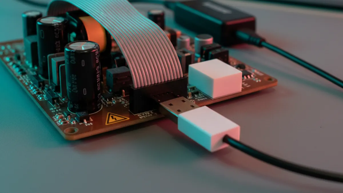
There is a failure mode that almost every embedded team in India runs into exactly once, and never forgets. An engineer is debugging a motor drive, a traction inverter, or a mains-connected power supply. The board is energized. The debug probe is plugged into the SWD or JTAG header, and its USB cable runs back to a laptop sitting on the same bench. Then something pops. Sometimes it is just the probe. Sometimes it is the laptop’s USB controller. In the worst case, the engineer was the lowest-resistance path between two grounds that should never have been connected.
The root cause is almost always the same: the debug host and the target were on different ground references, and the debug cable became the conductor that tied them together. The fix is galvanic isolation of the debug port: and SEGGER ships a small, fully specified family of isolators built for exactly this. This post explains what debug-port isolation actually means, why SEGGER sells separate target-side and host-side isolators, how isolation affects debug and trace speed, and how to choose the right combination. GSAS Micro Systems is an authorized engineering partner in India, every isolator and probe below is available in INR with local pre-sales engineering support.
What “debug-port isolation” actually means
Galvanic isolation lets two circuits exchange signals without any direct current flowing between them. The isolation barrier, built from digital isolators, optocouplers, or transformers, passes the logic information across while breaking the conductive path. SEGGER puts it plainly: with galvanic isolation, two circuits exchange signals without any direct current flow between them.
Why does a debug setup need this? SEGGER’s own isolator overview gives three concrete reasons:
- Ground loops. Development tools may not be connected to the same ground as the application. When the probe ties the host ground to a target ground that sits at a different potential, current flows where it should not.
- Electrical spikes. These often occur in motor-control applications, where switching transients can couple straight back up the debug cable into your probe and PC.
- Overvoltage and noise. Electrical noise from the development PC, and overvoltage from low-budget USB hubs, can damage the target side.
When the target’s ground is floating, mains-referenced, or sitting on a high-side / DC-bus potential: which is the normal state of affairs in power electronics, the only safe way to connect a grounded laptop is through an isolation barrier. That barrier is what stops a hazardous common-mode voltage on the target from ever reaching the probe, the PC, or the person holding the cable.
Two failure surfaces, two isolation layers
A debug connection has two distinct places it can go wrong, so SEGGER protects both with two different isolators:
- Target-side: between the probe and the target’s debug connector. This is where the JTAG, SWD, and J-Trace isolators sit. They protect the probe (and everything behind it) from the target’s potential.
- Host-side: between the PC and the probe. This is where the USB Isolator sits. It isolates the USB link itself, protecting both the probe and the host PC.
These are not redundant. They protect different surfaces. SEGGER explicitly recommends combining a host-side USB Isolator with a target-side JTAG/SWD isolator for high-voltage work. The target-side isolator keeps the target’s hazardous potential off the probe; the host-side isolator keeps any overvoltage that does reach the probe off your laptop. For motor control, inverters, and mains-connected supplies, you want both.
Target-side: SEGGER SWD Isolator (8.07.01)
The SEGGER SWD Isolator is the modern, digital-isolator-based choice for Arm Cortex-M bring-up. Verified specifications:
- Basic isolation of 1 kV DC
- SWD up to 4 MHz
- 1.2 V to 5 V target operation
- Target-side current consumption < 25 µA
- Built on high-speed digital isolators plus an isolated DC/DC converter that powers the target side across the barrier, both sides are totally isolated from each other
- 20-pin 0.1″ male connectors on both the emulator and target sides
- Ordering number 8.07.01
Because it uses digital isolators rather than optocouplers, it handles SWD’s bidirectional signalling cleanly and runs down to 1.2 V targets, useful for modern low-voltage SoCs.
Target-side: SEGGER JTAG Isolator (8.07.00) and why it cannot do SWD
The SEGGER JTAG Isolator is the optocoupler-based part for classic JTAG chains. Verified specifications:
- Basic isolation of 1 kV DC, built on high-speed optocouplers
- JTAG up to 4 MHz
- 3.3 V and 5 V target operation
- Target-side power draw 35 mA typical / 50 mA maximum
- Ordering number 8.07.00
Here is the important detail that trips up a lot of buyers: the JTAG Isolator cannot be used for SWD. SWD uses the TMS pin as a bidirectional pin, and the JTAG isolator’s optocoupler hardware does not support that bidirectional signalling. This is the concrete engineering reason SEGGER ships JTAG-only (8.07.00) and SWD-only (8.07.01) as separate parts rather than one combined isolator. If your target speaks SWD, as virtually every Cortex-M does, you need the SWD Isolator, not the JTAG one.
Note for buyers comparing pages: SEGGER’s catalog lists JTAG-only and SWD-only as distinct ordering numbers. Match the part to your interface, do not assume a single accessory covers both.
Host-side: SEGGER USB Isolator (8.07.02)
The SEGGER USB Isolator protects the host PC and the probe by isolating the USB link itself. Verified specifications:
- Basic isolation of 3 kV DC for 1 second
- Operates at USB Full-Speed (12 Mbit/s)
- 70 ns maximum propagation delay: to be treated as one additional USB hub
- 200 mA maximum output current, with overload protection
- USB Micro-B on the host side, USB Type-A on the device/Flasher side
- Green power LED plus a red overload LED that warns when the debug setup draws too much power
- Ordering number 8.07.02
SEGGER electrically separates the host from the J-Link and the target system here, protecting the J-Link and target hardware while also securing the host PC against overvoltage from the target. SEGGER recommends the USB Isolator specifically for motor control, inverter, and any high-voltage application, and, as noted above, to pair it with a target-side JTAG or SWD isolator.
High-speed trace through isolation: SEGGER J-Trace Isolator (8.07.10)
Isolation does not have to mean giving up parallel trace. The SEGGER J-Trace Isolator carries high-speed ETM trace across the barrier. Verified specifications:
- 1 kV DC isolation
- ETM trace pins (TRACECLK + TRACEDATA0–3) supported up to a 75 MHz trace clock
- JTAG and SWD control lines limited to 4 MHz
- .05″ 19-pin Cortex-M connector
- Compatible with J-Trace PRO V2 or later
- Ordering number 8.07.10
This is the standout capability of the family: you can keep full ETM instruction trace at a 75 MHz trace clock while sitting behind a 1 kV isolation barrier, the control interface drops to 4 MHz, but the trace pipe stays fast.
Need isolated high-speed trace? GSAS sources the SEGGER J-Trace Isolator (8.07.10) on request, contact us for a quote alongside your J-Trace PRO.
How isolation affects debug and programming speed
There is a real, sourced trade-off to plan around: crossing an isolation barrier costs interface clock speed. SEGGER’s SWD and JTAG isolators cap the debug interface at 4 MHz: well below what a bare J-Link can drive on the same target. That is the price of basic isolation on the control lines, and it applies to both the SWD Isolator and the JTAG Isolator.
For most bring-up work, 4 MHz is perfectly usable. Where it matters is high-volume flash programming and very large image downloads, where raw SWD/JTAG clock directly affects throughput. The practical workflow for Indian teams: do your isolated debugging and verification at 4 MHz on the energized, isolated bench, and run bulk programming on a de-energized board (or on a Flasher station configured for production) where appropriate.
The exception worth knowing is trace. The J-Trace Isolator preserves a 75 MHz trace clock across the barrier even while its JTAG/SWD control lines stay at 4 MHz. So if you are profiling control loops on an energized inverter and need cycle-accurate ETM trace, isolation does not force you to give up trace bandwidth, only the control-line clock is capped.
Where debug-port isolation is essential in Indian designs
Isolation moves from “nice to have” to “non-negotiable” wherever the target ground can sit at a hazardous or floating potential:
- Motor drives and inverters: switching transients couple straight up the debug cable; SEGGER calls out motor control by name as the canonical isolator use case.
- EV traction inverters and HV battery / BMS packs (400 V–800 V): the target ground may be referenced to a high-voltage DC bus. A grounded laptop has no business touching that without an isolation barrier. (General industry context, not a SEGGER spec: high-voltage motor controllers at 400 V and above require galvanic isolation between the probe and the PC precisely because the target ground may sit at a hazardous, mains- or DC-bus-referenced potential.)
- Mains-connected SMPS and grid-tied power gear: anything where the control MCU shares a ground with a rectified line voltage.
- Industrial drives and PLCs: long cable runs and multiple earth references make ground loops the default state, not the exception.
- Noisy production lines: where ground-loop-induced glitches show up as intermittent programming failures.
An honest safety note: basic vs reinforced isolation
This part matters, and it is where careless marketing gets companies into trouble. SEGGER classifies all of these isolators as BASIC isolation only: 1 kV DC on the target side, 3 kV DC on the host side. They are not reinforced and not medical-grade. SEGGER’s SWD Isolator page warns directly that it provides basic isolation only and must not be used with hazardous voltages without further protection measures.
For context, and only as background, medical device isolation under IEC 60601-1 defines far higher reinforced requirements (for example, 2× MOPP corresponds to roughly 4000 V AC isolation, with greater creepage and double insulation). That standard exists to protect patients in direct contact with equipment. SEGGER’s basic debug isolators are not a substitute for certified medical isolation, and nothing in this post should be read as claiming they meet IEC 60601. If you are building patient-contact equipment, the debug isolator is a development-bench safety tool, not part of your product’s clinical isolation strategy, treat the two as completely separate engineering problems.
We also flag the figures we could not independently verify on segger.com so you do not over-specify: exact working-voltage vs test-voltage breakdowns, creepage/clearance distances, and physical dimensions/weight for the JTAG and SWD isolators. If your safety case needs those numbers, ask GSAS and we will confirm them with SEGGER before you commit.
Production programming: Flasher plus isolators
The same isolators that protect a debug bench protect a production line. SEGGER’s Flasher isolators are not separate products: the isolator family (JTAG, SWD, USB) is a single unified line shared across the Flasher, J-Link, and J-Trace probes. The same 1 kV DC target-side and 3 kV DC host-side isolators used on the bench are used in production to break ground loops and protect programming equipment from spikes when programming motor-control and high-voltage targets. For Indian contract manufacturers and EMS lines, this means one consistent isolation strategy from first bring-up through volume programming.
Choosing the right isolator: a quick decision guide
| Isolator | Interface | Isolation (verified) | Max interface speed | Where it sits | What it protects |
|---|---|---|---|---|---|
| SWD Isolator (8.07.01) | SWD, 1.2–5 V | 1 kV DC basic | SWD up to 4 MHz | Target-side (probe → board) | Probe + everything behind it |
| JTAG Isolator (8.07.00) | JTAG only, 3.3/5 V | 1 kV DC basic | JTAG up to 4 MHz | Target-side (probe → board) | Probe; cannot do SWD (bidirectional TMS) |
| USB Isolator (8.07.02) | USB Full-Speed | 3 kV DC basic (1 s) | 12 Mbit/s, +70 ns delay | Host-side (PC → probe) | Host PC + probe |
| J-Trace Isolator (8.07.10) | JTAG/SWD + ETM trace | 1 kV DC basic | Trace 75 MHz; JTAG/SWD 4 MHz | Target-side (probe → board) | Probe, while keeping parallel trace |
For high-voltage work, the SEGGER-recommended combination is a host-side USB Isolator plus a target-side SWD (or JTAG) isolator: two layers, two failure surfaces covered.
Pair the isolation with the right probe
An isolator is only half the setup; behind it you need a J-Link suited to the job:
- J-Link PLUS: the practical choice for bench bring-up and isolated single-target debugging.
- J-Link PRO: the flagship probe for lab and production setups, including networked and shared-bench scenarios.
Confirm the exact probe speed figures on segger.com before quoting any download numbers, the verified isolated-debug figure to rely on is the isolator’s 4 MHz control-line cap, not the bare probe’s headline speed.
Frequently asked questions
Do I need both a target-side and a host-side isolator? For high-voltage targets (motor drives, inverters, HV battery packs), yes, SEGGER recommends pairing the host-side USB Isolator (8.07.02) with a target-side SWD or JTAG isolator. They protect different failure surfaces: the target-side keeps the target’s potential off the probe, the host-side keeps overvoltage off your PC.
Can the SEGGER JTAG Isolator be used for SWD? No. The JTAG Isolator (8.07.00) cannot do SWD because SWD uses the TMS pin bidirectionally, which the optocoupler hardware does not support. Use the SWD Isolator (8.07.01) for SWD targets.
How much does isolation slow down debugging? The SWD and JTAG isolators cap the control interface at 4 MHz. That is lower than a bare J-Link but fine for most bring-up. The exception is the J-Trace Isolator, which keeps ETM parallel trace at a 75 MHz trace clock while its JTAG/SWD lines stay at 4 MHz.
Are SEGGER isolators safe for medical (IEC 60601) applications? No. SEGGER classifies these as basic isolation only (1 kV DC target-side, 3 kV DC host-side), explicitly not reinforced or medical-grade. They are a development-bench safety tool and are not a substitute for certified medical isolation under IEC 60601-1.
Are the Flasher isolators different from the J-Link isolators? No. SEGGER’s isolator line (JTAG, SWD, USB) is one unified family shared across the Flasher, J-Link, and J-Trace probes. The same parts protect both your debug bench and your production programming station.
Why GSAS for SEGGER isolation in India
Specifying debug-port isolation is not a catalog-picking exercise, it is an engineering decision about which failure surfaces you are exposing and how your target’s ground is referenced. As an authorized SEGGER engineering partner in India, GSAS Micro Systems helps you choose the correct host-side plus target-side isolation combination for your motor drive, inverter, EV battery, or industrial design, supplies the J-Link, J-Trace, and Flasher hardware behind it, and quotes everything in INR with GST. Our pre-sales engineers work hands-on with teams across Bengaluru, Hyderabad, Chennai, Pune, Mumbai, and Delhi NCR: from first energized bring-up to volume production programming. Request a quote or book a demo on your own target hardware, and see the full SEGGER range on our SEGGER partner page.
Further reading
- SEGGER isolators overview, the canonical source for the isolator family
- SEGGER SWD Isolator (8.07.01), target-side digital isolation
- SEGGER USB Isolator (8.07.02), host-side USB isolation
- SEGGER J-Trace Isolator (8.07.10), isolated high-speed trace
- GSAS J-Link & Flasher isolators, buy in India through GSAS
Also appears in:
Interested in SEGGER tools?
Talk to our application engineers for personalized tool recommendations.
More from SEGGER
View all →
Meet the GSAS Team at electronica India 2026, Stall H3.I45
15 Sept · 3 min
J-Link Is Now Validated by ST for StellarStudio
13 Sept · 2 min
An AI Agent That Drives the Debugger: SEGGER and Embedder Connect J-Link to the Loop
13 Sept · 6 min
SEGGER J-Link and J-Trace Now Support Andes Trace: Why This Matters for RISC-V
21 Jul · 6 min

Emulating Processor Power for Thermal Testing: Why Constant Power
7 Oct · 7 min

CRPS and Rack Power Supply Testing: The Six Tests That Matter
7 Oct · 7 min