In short
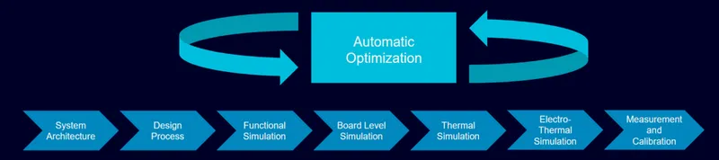
Siemens EDA's HyperLynx power electronics workflow replaces trial and error with continuous verification: HyperLynx Schematic Analysis checks the design concept, HyperLynx AMS simulates the switch-mode supply and explores values with DSE, the Advanced Solver extracts board parasitics, HyperLynx SI/PI checks the PDN, and thermal and electro-thermal simulation close the loop.
Power electronics now sits under almost everything: network switches, electric vehicles, industrial controls. And it fails on details. A December 2025 Siemens EDA article lists the usual suspects: a poorly chosen PCB stack-up, a switch-mode power supply operated outside its recommended range, sub-optimal capacitor selection, and thermal stress nobody modelled. Each is cheap to fix at the concept stage and expensive once hardware exists.
The traditional answer is to build, measure, adjust and build again.

Siemens’ article lays out the alternative as a sequence of HyperLynx steps in which simulation and verification run continuously from the first schematic. This post follows that sequence. The original article is linked under References.
Step 1: Design process
The flow starts from an integrated schematic and an enterprise shared component library that links electrical, physical and manufacturing data from the moment a part is created. HyperLynx Schematic Analysis checks that schematic for consistency and validates the design concept before any hardware exists.
Step 2: Functional simulation
With a validated schematic, HyperLynx AMS simulates the switch-mode power supply (SMPS) in both the time and frequency domains, for example to set the feedback resistor values and optimise the output voltage. The combined simulation shows losses and power dissipation, which characterises the SMPS well enough to model the voltage regulator module (VRM) in the later board-level analysis.
From HyperLynx 2510, Design Space Exploration (DSE) can be launched directly from HyperLynx AMS to explore what-if scenarios, such as constraints on feedback resistor values and current. Our DSE explainer covers how that search works.
Candidate routing and placement options are then verified with the HyperLynx Advanced Solver, which automates parasitic extraction. Board parasitics such as resistance, inductance and conductance are back-annotated to the schematic, so the simulation shows how the real board affects switching behaviour and predicts electrical losses more accurately.
Step 3: Board-level simulation
HyperLynx SI/PI runs an AC analysis of PDN impedance over frequency, now including the extracted board parasitics. Siemens positions HyperLynx SI/PI as the centrepiece of PDN work: DC drop analysis, AC decoupling analysis and PDN optimisation. For a worked PDN example on a real board, see our post on HyperLynx PI for AMD Versal devices.
Step 4: Thermal and electro-thermal simulation
HyperLynx integrates with mechanical and thermal co-simulation tools, so engineers can analyse how heat build-up interacts with electrical behaviour and test placement strategies for heat-sensitive parts.
Siemens says HyperLynx also brings stack-up checks, dynamic-response modelling of switch-mode regulators, and work that used to need scripts (design space exploration, capacitor checks, power maps, AC and DC analysis) into one automated electro-thermal workflow, correlated against measured data.
The example Siemens uses
Siemens illustrates the integrated approach with a Microchip switch reference design, the KSZ9477. Automated design exploration identified candidate solutions, routing and placement were introduced, and the changes were verified with a 3D EM solver. Siemens reports that this produced an optimised placement, reduced switching losses, and met the design requirements.
Why it matters for Indian power electronics teams
EV chargers and drivetrains, solar inverters, industrial drives and data-centre power are all active development areas in India, and they share one trait: the first prototype is expensive, and the second one costs schedule. A workflow that verifies the supply, the board and its thermal behaviour before hardware is a direct way to cut the number of spins. For the PDN and wide-bandgap side of the same problem, see our earlier post on power electronics PCB design with HyperLynx.
Working with GSAS
GSAS supports the Siemens EDA portfolio in India, HyperLynx included, with local application engineers who can map the HyperLynx steps of this workflow onto your next power design. Talk to us from Bengaluru, Hyderabad, Chennai, Pune, Mumbai or Delhi NCR.
References
- Siemens EDA, Electronic Systems Design blog: How our customers are transforming power electronics design with HyperLynx for true design optimization (9 December 2025)
- Siemens EDA: HyperLynx Schematic Analysis, HyperLynx AMS, HyperLynx Power Integrity
- HyperLynx and the Siemens EDA partner page at GSAS
Also appears in:
Interested in Siemens EDA tools?
Talk to our application engineers for personalized tool recommendations.
More from Siemens EDA
View all →
HyperLynx 2610: What's New for India's Signal and Power Integrity Teams
4 Nov · 6 min
Simulation-Based FMEDA: HyperLynx AMS and Xpedition in the Functional Safety Workflow
4 Nov · 5 min
FMI Co-Simulation in HyperLynx AMS and PartQuest Explore: Electrical, Mechanical and Thermal Models in One Run
4 Nov · 5 min
HyperLynx DSE: Searching Millions of PCB "What If" Scenarios Without Simulating Them All
4 Nov · 5 min
Right-Sizing Decoupling on AMD Versal Boards with HyperLynx PI
4 Nov · 5 min

Keil Studio for VS Code: A Four-Part GSAS Webinar Series for Cortex-M Teams
4 Nov · 5 min