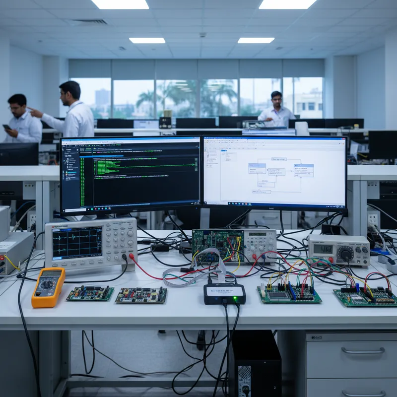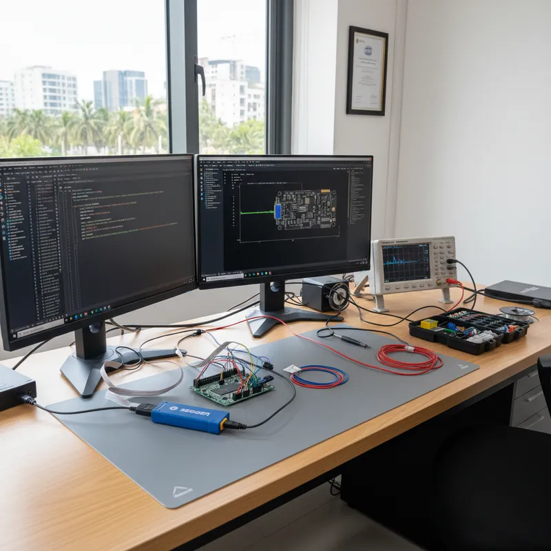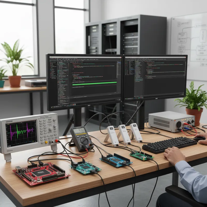
Every interesting Cortex-M chip shipped in the last three years is dual-core. NXP’s i.MX RT1170 pairs a 1 GHz Cortex-M7 with a 400 MHz Cortex-M4, and the combination now sits at the heart of Indian vision-system controllers, smart appliances, and industrial HMI. Nordic Semiconductor’s nRF5340 runs an application-core Cortex-M33 alongside a network-core Cortex-M33 dedicated to the BLE/Thread/Matter radio protocol stack, and shows up in every new Indian wearable, smart-home, and asset-tracking design. Raspberry Pi’s RP2350 is dual Cortex-M33 plus dual RISC-V Hazard3 cores, selectable at boot, and is increasingly the choice for cost-sensitive Indian consumer electronics moving up from RP2040.
All of these designs have one thing in common beyond the core count: the multi-core interaction is where real bugs live, and single-core debug tutorials, which is all the public Indian content covers, do not tell you how to find them. This post walks through the J-Link and Ozone multi-core debug workflow end-to-end. It is based on SEGGER’s J-Link multi-core debugging technology and the practical experience GSAS engineers have gathered debugging Indian product teams’ dual-core builds. GSAS Micro Systems is an authorized SEGGER engineering partner in India, every J-Link and J-Trace variant is available with INR invoicing across 11 offices across India.
Why multi-core debug is qualitatively different
On a single-core Cortex-M, debug is straightforward: one program counter, one call stack, one set of registers, one debugger attached to one probe. When a bug happens, you halt the core, inspect state, and step back through the execution. The mental model is linear.
On a dual-core system, debug is a coordination problem. Bugs live in the interaction: two cores stepping through shared memory at slightly different rates, one core stalling while the other hits a deadline, a message queue from the application core filling up because the network core stopped draining it, a mutex held by core A while core B waits in an ISR that will never retire. Halting one core does not halt the other, which means by the time you look at the “paused” state, the other core has moved on and the bug is gone. The mental model is not linear; it is concurrent, and the debugger needs to match that.
J-Link and the SEGGER software stack are designed for this concurrent model. A single J-Link probe connects to both cores of an i.MX RT1170, an nRF5340, an RP2350, or any other supported dual-core target. Ozone opens two debug sessions from the same probe, one per core, with independent breakpoints, independent call stacks, independent register views, and synchronized run-control that halts both cores simultaneously when any one of them hits a stop condition.
The J-Link connection model: one probe, multiple cores
Physically, every dual-core chip in scope here has a single JTAG/SWD debug port exposed on a single connector. The J-Link firmware enumerates the targets behind that port as a daisy-chained or logical-multiplex set, and each core gets its own debug session identity (called a “select” in SEGGER terminology). The J-Link GDB server can be launched multiple times, once per core, each instance pointing at the same J-Link but at a different core.
For i.MX RT1170:
- Cortex-M7 at 1 GHz, application core, runs the main application firmware (vision, HMI, control).
- Cortex-M4 at 400 MHz, co-processor core, typically runs a real-time loop (motor drive, sensor acquisition, simple protocol).
- Both cores connect via the same JTAG/SWD connector; J-Link presents them as two separate debug targets.
For nRF5340:
- Application core Cortex-M33 at 128 MHz, runs application firmware.
- Network core Cortex-M33 at 64 MHz, runs Nordic’s BLE/Thread/Matter protocol stack and is normally not user-modifiable (Nordic ships a pre-compiled network-core image).
- Access to the network core for debug is possible but requires understanding that you are debugging Nordic’s firmware, not your own.
For RP2350:
- Dual Cortex-M33 at 150 MHz, or dual RISC-V Hazard3 at 150 MHz, switchable at boot via a platform register.
- Both cores run user firmware symmetrically (unlike RT1170, which has a clear application/co-processor split).
- J-Link supports both Arm and RISC-V modes on RP2350 from the same physical probe, pick your architecture via an Ozone / GDB server configuration flag.
The Ozone multi-core workflow: the concrete session
Ozone is SEGGER’s standalone graphical debugger, and it is the tool that makes multi-core debug approachable rather than painful. The practical Indian engineer workflow:
- Launch two Ozone instances pointing at the same ELF project (or two ELF projects, one per core, for RT1170’s typical M7+M4 split where the two cores run different firmware). Each instance is configured for one core.
- Set breakpoints in both instances. Ozone gives each core its own breakpoint list. Put a breakpoint on the M7 application core’s event-handler entry and another on the M4 co-processor’s ISR, and when you run the system, both cores will halt at their respective breakpoints.
- Enable synchronized run-control. Ozone’s “sync halt” mode tells the J-Link to halt both cores the moment either one stops. This is what turns multi-core debug from “try to catch both cores at the same moment by hand” into a coherent stepping experience.
- Use the two Ozone timeline views side by side. The Ozone execution timeline (fed by SystemView instrumentation or by J-Trace trace streaming) shows each core’s activity on a common time axis. Bugs that were previously invisible, “the M4 starved because the M7 took a mutex and got preempted by an ISR that never returned”, become obvious.
- RTT log channels for each core, on the same J-Link. RTT supports multiple channels. Assign channel 0 to the M7’s printf stream and channel 1 to the M4’s printf stream. The J-Link RTT Viewer (or two separate viewer instances) displays both in real time, with matching timestamps, and gives you the human-readable narrative of what each core was doing when the bug manifested.
For the synchronized halt to work, the J-Link needs appropriate firmware (any recent J-Link Software Pack release includes it) and the target needs debug signals routed cleanly to both cores. On custom boards, verify that the JTAG/SWD connector is wired according to the silicon vendor’s reference schematic, multi-core debug is where the “I saved two traces by not routing that signal” decision comes back to hurt.
J-Link model selection for multi-core work
Every J-Link supports multi-core debug in principle, but the practical choice for Indian teams running this workflow daily is:
- J-Link BASE Compact: sufficient for bench work. Works fine for i.MX RT1170, nRF5340, RP2350. Entry point.
- J-Link PLUS: adds the unlimited flash breakpoints license on top of BASE. The right choice if your team is shipping a commercial product and needs breakpoint headroom across two cores’ interrupt handlers and RTOS code.
- J-Link ULTRA: USB 2.0 Hi-Speed with download speeds up to 4 MB/s and high-speed RTT. This is the recommended model for serious multi-core debug work: the RTT throughput matters when both cores are logging simultaneously, and the 4 MB/s download speed cuts iteration time on large-firmware builds (common on i.MX RT1170 with external flash).
- J-Link PRO: Ethernet interface. Essential for CI/CD racks where the dual-core target needs to be flashed and tested from a build server over LAN. For any bench where the target runs at voltages that warrant electrical isolation, pair the probe with the separate SEGGER J-Link Isolator; galvanic isolation is not built into the probe itself.
- J-Trace PRO Cortex-M: streaming ETM trace. For Indian automotive and safety-critical medical teams who need full instruction-by-instruction execution capture across both cores simultaneously, J-Trace PRO is the only tool that delivers it. More expensive than J-Link PRO, justified only when instruction trace is specifically required.
Per-silicon debugging notes
i.MX RT1170, M7 + M4 with XIP from external flash. The RT1170 executes application code from external Octo-SPI or HyperFlash, which introduces a subtlety: when you flash the firmware, you are really flashing the external memory, not the MCU’s on-chip flash. SEGGER’s J-Flash handles this cleanly, but the first-time bring-up on a custom RT1170 board is where Indian teams most often get stuck, the flash loader needs the specific external memory part in its device database, and if the part is not in the stock list, you need to generate a custom flash loader script. GSAS can help with this step; it is a one-time cost per board design.
nRF5340, application core + network core with SoftDevice protocol stack. The nRF5340’s network core normally runs Nordic’s pre-compiled BLE/Thread/Matter firmware, and debugging it is limited to what Nordic exposes through their source code in the Nordic Connect SDK. For almost all Indian product work, you debug only the application core and treat the network core as a black box, J-Link still attaches cleanly, but Ozone’s stepping and breakpointing on the network core is unlikely to be useful unless you are specifically working on Nordic’s network stack. The one case where network-core debug matters in practice is when a BLE timing problem is suspected, SystemView on the application core, correlated with the network core’s RTT log stream, is the path to isolate it.
RP2350, dual Cortex-M33 with mode switch to dual RISC-V Hazard3. RP2350’s architecture selection happens at boot time via the OTP fuses; once committed, the chip is in Arm mode or RISC-V mode for its lifetime. For debug, J-Link supports both modes, but you need to know which mode the target is in before attaching, attaching an Arm debug session to a RISC-V-mode chip fails immediately. In the Ozone project settings, the architecture is a configuration option on the target profile. Indian teams evaluating RP2350 for cost-sensitive designs should commit to one mode early and run the full debug workflow on that mode before going to production.
Multi-core application debug patterns that matter
Beyond the mechanical “how do I attach to both cores” question, the workflow patterns that save Indian teams time on dual-core builds:
- Core-identified logging. Tag every RTT log message with a core ID (
[M7],[M4],[APP],[NET]) so the two log streams can be merged into one timeline without ambiguity about which core emitted which line. - Shared-memory invariant checks. When two cores share a data structure (a ring buffer, a command queue, a sensor reading), have each core’s debug build independently assert the invariants on every read and write, not just on the writer side. Mismatches between the writer’s view and the reader’s view are where concurrency bugs live.
- Synchronized time base. Configure both cores to read from a common hardware timer (LPTIM or RTC on STM32, the global TIMER on nRF5340, the SYSTICK combined with a GPT on RT1170) and timestamp every RTT log entry with the shared time. When you replay the logs post-capture, both cores’ events align on one axis.
- One-core-at-a-time tests. During bring-up, run tests with only one core enabled at a time. This is not the final test environment, but it isolates single-core bugs from multi-core coordination bugs and lets the team fix each class independently.
Ordering the right J-Link for multi-core work in India
GSAS is an authorised SEGGER engineering partner in India and supplies the J-Link family on quote. For Indian teams starting a new i.MX RT1170 / nRF5340 / RP2350 project, the typical first purchase is a J-Link PLUS or J-Link ULTRA for the lead firmware engineer’s bench, expanding to J-Link PRO for the CI/CD rack when the team moves into integration testing. Contact GSAS for model selection guidance specific to your target silicon and a hands-on multi-core debug session at any of our 11 offices across India.
Further reading
- SEGGER J-Link Multi-Core Debugging technology
- SEGGER Ozone standalone debugger
- SystemView V4, ELF-based timeline analysis, critical companion tool for multi-core timeline analysis
- SEGGER J-Link with NXP i.MX RT crossover MCUs, single-core workflow on the same silicon family
- SEGGER J-Link with Nordic nRF52/nRF53, Nordic-specific debug workflow
- SEGGER J-Link with Raspberry Pi RP2040/RP2350, RP2xxx workflow
- Buying the right J-Link for your project
- SEGGER at GSAS
Interested in SEGGER tools?
Talk to our application engineers for personalized tool recommendations.
More from SEGGER
View all →
Meet the GSAS Team at electronica India 2026, Stall H3.I45
15 Sept · 3 min
J-Link Is Now Validated by ST for StellarStudio
13 Sept · 2 min
An AI Agent That Drives the Debugger: SEGGER and Embedder Connect J-Link to the Loop
13 Sept · 6 min

SEGGER J-Link and J-Trace Now Support Andes Trace: Why This Matters for RISC-V
21 Jul · 6 min

Emulating Processor Power for Thermal Testing: Why Constant Power
7 Oct · 7 min

CRPS and Rack Power Supply Testing: The Six Tests That Matter
7 Oct · 7 min