Sensepeek SQG Series: Passive 6 GHz Probes for Signal Integrity and RF Debugging
The SQ-series oscilloscope probes in the Sensepeek PCBite ecosystem top out at 500 MHz, sufficient for most embedded debugging, but nowhere near enough for signal integrity validation on multi-gigabit serial interfaces. The SQG series fills that gap with passive 10:1 probes spanning 1.5 GHz, 3 GHz, and 6 GHz bandwidths, designed for 50-ohm instrument environments and delivered in the same hands-free PCBite form factor.
This post covers the three SQG models, when each is appropriate, and what makes them different from the SQ-series probes they complement.
The SQG Family at a Glance
| Parameter | SQG15 | SQG30 | SQG60 |
|---|---|---|---|
| Bandwidth (-3 dB) | 1.5 GHz | 3 GHz | 6 GHz |
| Attenuation | 10:1 | 10:1 | 10:1 |
| Probe Tip Impedance | 500 ohm | 500 ohm | 500 ohm |
| Rise Time | < 190 ps | < 103 ps | - |
| Tip Capacitance | 1.36 pF | 0.35 pF | Ultra-low |
| Connector | SMA (50 ohm) | SMA (50 ohm) | SMA (50 ohm) |
| Variants | AC, DC | AC, DC | AC, DC |
| Ground Options | 2.3 mm dual + 6.5 mm single | 2.3 mm dual + 6.5 mm single | 2.3 mm dual + 6.5 mm single |
All three models share a common architecture: passive 10:1 attenuation with 500-ohm probe tip impedance, SMA output for 50-ohm instruments, and the same PCBite magnetic mounting system. Each is available in AC-coupled and DC-coupled variants.
Why Passive at GHz Frequencies?
Active probes have historically dominated the GHz probing space, but they come with tradeoffs: limited dynamic range, higher noise floors, susceptibility to ESD damage, and significant cost. The SQG series takes a passive approach that offers high dynamic range, low noise, superior linearity, and long-term stability in signal flatness. For signal integrity characterization where you need to see the true waveform without probe-induced artifacts, these attributes matter.
The 500-ohm probe tip impedance is a deliberate design choice. It sits between the 10 M-ohm of the SQ-series (which becomes ineffective above a few hundred MHz due to parasitic capacitance) and the 50-ohm of traditional transmission-line probes (which would load high-impedance nodes). At 500 ohms, the SQG probes provide enough isolation to probe signal traces without collapsing the signal, while maintaining flat frequency response into the GHz range.
Choosing Your Bandwidth Tier
SQG15: 1.5 GHz
The SQG15 with sub-190 ps rise time and 1.36 pF tip capacitance handles data rates up to approximately 3 Gbps. Practical applications include USB 2.0 eye diagram characterization, Gigabit Ethernet PHY debugging, SATA Gen 1 signal quality validation, and clock distribution analysis for PLL jitter measurements. At ±0.5 dB flatness from DC to 1.5 GHz, the SQG15 provides honest frequency response for pre-compliance checks.
For hardware teams in Bengaluru and Hyderabad working on networking equipment or industrial Ethernet systems, the SQG15 covers the most common high-speed interfaces without over-investing in bandwidth.
SQG30: 3 GHz
The SQG30 extends to 3 GHz with sub-103 ps rise time and an exceptionally low 0.35 pF tip capacitance, the lowest capacitive loading in the SQG family. At 3 GHz bandwidth, the SQG30 captures signals at data rates up to 6 Gbps fundamental. Target applications include USB 3.0 (5 Gbps), PCIe Gen 2/3, HDMI 1.4, SATA Gen 2/3, and high-speed DDR memory interface validation.
The extremely low tip capacitance makes the SQG30 particularly well-suited for probing high-impedance transmission line structures where even small capacitive loads cause reflections and distort the measurement.
SQG60: 6 GHz
The SQG60 is the highest-bandwidth probe in the entire PCBite ecosystem. At 6 GHz, it covers USB 3.x, PCIe Gen 3/4, HDMI 2.0, and 5G NR front-end characterization. The SQG60 is the right choice for teams validating multi-gigabit interfaces, RF circuits, or any signal path where frequency content extends beyond 3 GHz.
For design centers in Chennai and Pune working on advanced consumer electronics, telecom baseband processing, or high-speed SerDes validation, the SQG60 provides desktop-grade high-frequency probing capability.
AC vs DC Coupling: When Each Matters
Every SQG model comes in two variants:
DC-coupled (SQG15-DC, SQG30-DC, SQG60-DC) passes the full signal including its DC offset. Use DC coupling when you need to measure absolute voltage levels, assess DC bias points on active circuits, or characterize signals where the DC component carries information. The SQG15-DC, for example, supports 16.4 V RMS continuous input voltage.
AC-coupled (SQG15-AC, SQG30-AC, SQG60-AC) blocks the DC component and passes only signal transitions. Use AC coupling when you are focused on signal quality, eye diagrams, jitter, rise/fall times, and the DC operating point is irrelevant or would saturate your oscilloscope’s input range. AC coupling is standard practice for compliance-style eye diagram measurements.
Ground Options for RF Board Layouts
Clean ground contact is critical at GHz frequencies. The SQG probes provide two ground options: a 2.3 mm dual-needle ground designed for closely spaced PCB-mounted RF connectors and component ground pads, and a 6.5 mm single ground spring for wider pin spacing. Selecting the shorter ground path minimizes ground loop inductance and improves measurement accuracy, a detail that matters when characterizing edge rates below 100 ps.
Why Buy from GSAS
GSAS is an authorized engineering partner in India, providing the full SQG probe family with INR invoicing and local application support. Our engineers in Bengaluru, Hyderabad, Chennai, Pune, and Mumbai help teams select the right bandwidth tier and coupling variant for their specific signal integrity or RF validation requirements. We stock evaluation units and can arrange hands-on demonstrations. Contact GSAS for pricing on SQG probes and complete PCBite kits.
Also appears in:
Interested in Sensepeek tools?
Talk to our application engineers for personalized tool recommendations.
More from Sensepeek
View all →
Shrinking Boards, Growing Problems: Why Hands-Free Probing Is Essential as Component Density Rises
7 Apr · 4 min

Getting Started with Sensepeek PCBite: Unboxing to First Measurement
7 Apr · 5 min
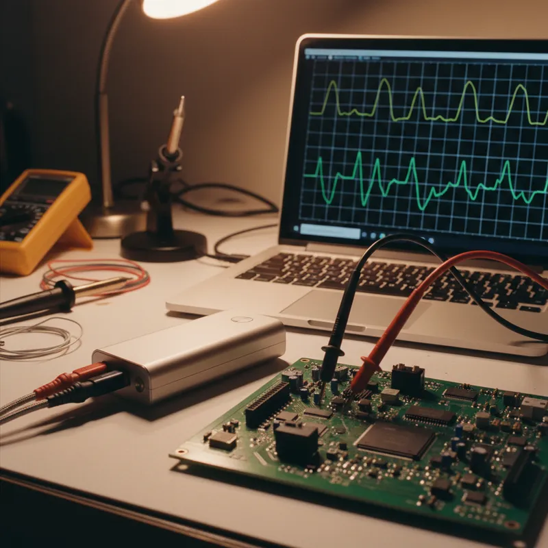
High-Speed Interface Validation with Sensepeek SQG Probes: USB, HDMI, and SATA
7 Apr · 5 min
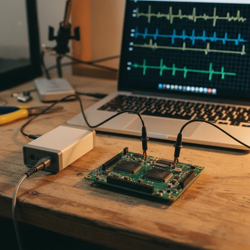
6 Simultaneous Probe Points: Multi-Point Measurement with Sensepeek PCBite
7 Apr · 4 min

Emulating Processor Power for Thermal Testing: Why Constant Power
7 Oct · 7 min

CRPS and Rack Power Supply Testing: The Six Tests That Matter
7 Oct · 7 min